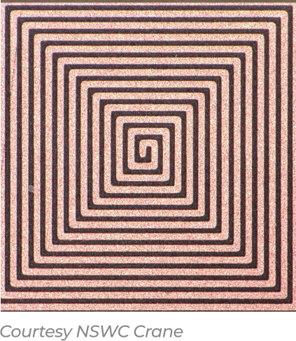
A very high density patented manufacturing process for circuit boards with metal traces as narrow as 15 microns.
Benefits
Reduction in size and weight by 90% over current state-of-the-art in the US
Effectively reduce layer count and lamination cycles
Significant RF advantages over traditional subtractive etch processes
Increased electronics density within a fixed area
A-SAP™ sub 15 μm trace/space
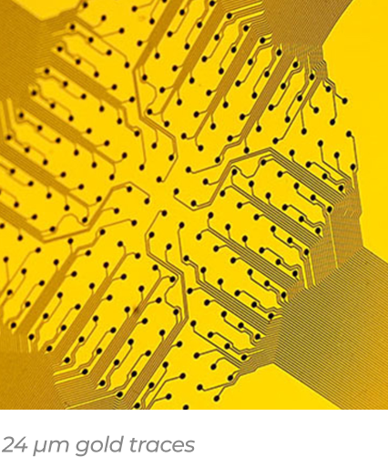
24 μm gold circuit neural probe
Ideal for Medical and Healthcare applications
Using gold as conductive metal
Utilizing only bio compatible materials for applications such as neural probes, glucose monitoring and other implantable devices
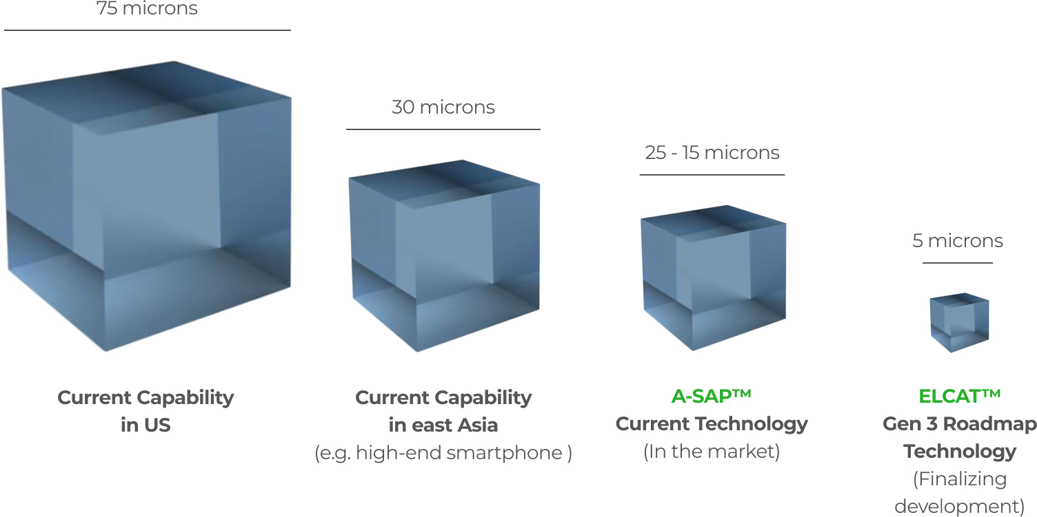
Relative Miniaturization Capability
Small is better. Cubes represent proportional volumetric size various electronic connection alternatives.
Averatek A-SAP™ allows use of much smaller packages
Immediate benefit of using A-SAP™ for domestic vendors
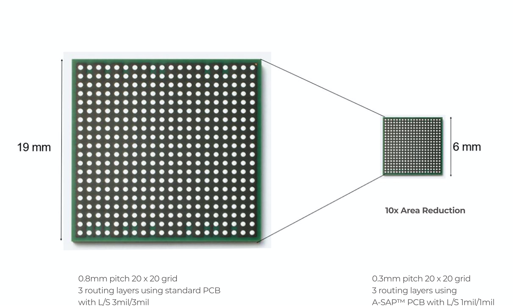
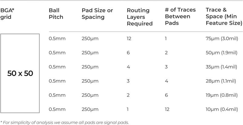
Smaller Trace/Space Size Reduces Layer Count
A-SAP™
High Frequency Benefits:
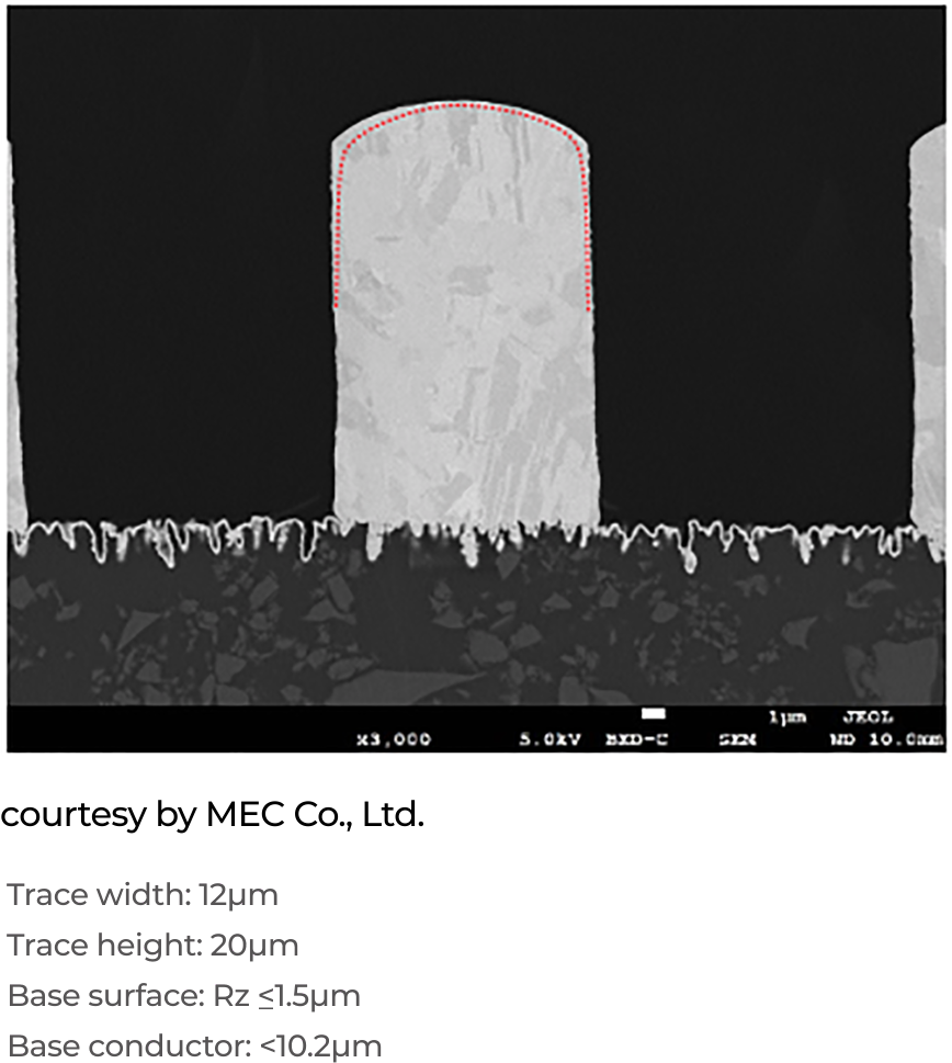
Vertical Walls
Tight Tolerances
Improved Impedance Control
Averatek Semi-Additive Process (A-SAP™)
Easily implemented in traditional PCB shops.
Utilizing proprietary semi-additive processing techniques, a very thin layer of electroless copper enables PCB fabricators to realize fine pitch feature sizes at 15 micron trace and space and below while integrating with traditional PCB fabrication equipment.